FESEM vs SEM vs TEM: Which Electron Microscopy Technique Should You Choose?
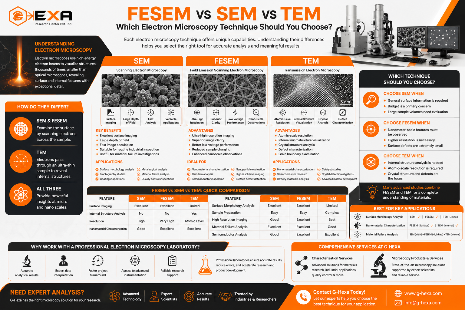
Modern materials research, semiconductor development, nanotechnology innovation, and industrial quality control all depend on advanced imaging techniques to understand materials at microscopic and nanoscopic scales. Among the most widely used methods are Field Emission Scanning Electron Microscopy (FESEM), Scanning Electron Microscopy (SEM), and Transmission Electron Microscopy (TEM).
While all three techniques fall under the umbrella of electron microscopy, each serves a unique purpose and provides different types of information. Choosing the right technique can significantly impact the accuracy, speed, and value of your research results.
In this guide, we’ll compare FESEM, SEM, and TEM to help researchers, manufacturers, and engineers determine the most suitable approach for their analytical needs.
Understanding Electron Microscopy
Traditional optical microscopes are limited by the wavelength of visible light. Electron microscopes use high-energy electron beams instead of light, allowing scientists to visualize structures thousands of times smaller than what optical microscopes can resolve.
Advanced Electron Microscopy Services help researchers investigate material structure, composition, defects, and nanoscale features that are invisible using conventional imaging techniques.
What is SEM Analysis?
Scanning Electron Microscopy (SEM) uses a focused electron beam to scan the surface of a specimen. As electrons interact with the material, detectors collect signals that generate highly detailed images of surface structures.
Key Benefits of SEM Analysis
- Excellent surface imaging
- Large depth of field
- Fast image acquisition
- Suitable for routine industrial inspection
- Useful for material failure investigations
Applications of SEM Analysis
- Surface Morphology Analysis
- Fractography studies
- Coating inspections
- Metallurgical analysis
- Material Failure Analysis
- Quality control inspections
SEM is often the first choice when researchers need general surface information and structural evaluation.
Learn more about professional SEM and FESEM Analysis Services for industrial and research applications.
What is FESEM Analysis?
Field Emission Scanning Electron Microscopy (FESEM) is an advanced version of conventional SEM. Instead of using a thermionic electron source, FESEM utilizes a field emission gun that produces a much finer and brighter electron beam.
This enhancement significantly improves image resolution and enables visualization of extremely small nanostructures.
Advantages of FESEM Analysis
- Ultra-high resolution imaging
- Superior image clarity
- Better low-voltage performance
- Reduced sample charging
- Enhanced nanoscale observations
When Should You Choose FESEM Testing?
FESEM Testing is ideal when your research requires:
- Nanomaterial Characterization
- Thin-film analysis
- Semiconductor inspection
- Nanoparticle evaluation
- High Resolution Imaging
- Surface defect detection
Researchers studying advanced materials frequently rely on FESEM Analysis because of its ability to reveal intricate nanoscale features with exceptional detail.
What is TEM Analysis?
Transmission Electron Microscopy (TEM) differs fundamentally from SEM and FESEM.
Instead of scanning a material’s surface, TEM transmits electrons through an ultra-thin sample. The resulting image reveals internal structures at atomic and crystallographic levels.
Advantages of TEM Analysis
- Atomic-scale resolution
- Internal microstructure visualization
- Crystal structure analysis
- Defect characterization
- Grain boundary examination
Applications of TEM Analysis
- Nanomaterial Characterization
- Semiconductor research
- Battery materials analysis
- Catalyst studies
- Crystal defect investigations
- Advanced material development
Researchers seeking atomic-level insights often choose TEM Analysis Services for detailed structural investigations.
FESEM vs SEM vs TEM: Quick Comparison
| Feature | SEM | FESEM | TEM |
|---|---|---|---|
| Surface Imaging | Excellent | Excellent | Limited |
| Internal Structure Analysis | No | No | Yes |
| Resolution | High | Very High | Atomic Level |
| Nanomaterial Characterization | Good | Excellent | Excellent |
| Surface Morphology Analysis | Excellent | Excellent | Limited |
| Sample Preparation | Easy | Easy | Complex |
| High Resolution Imaging | Good | Excellent | Best |
| Material Failure Analysis | Excellent | Excellent | Good |
| Semiconductor Analysis | Good | Excellent | Excellent |
Which Technique is Best for Surface Morphology Analysis?
If your objective is Surface Morphology Analysis, both SEM and FESEM are excellent options.
Choose SEM when:
- General surface information is required
- Budget is a primary concern
- Large sample volumes need evaluation
Choose FESEM when:
- Nanometer-scale features must be observed
- Higher resolution is necessary
- Surface defects are extremely small
For advanced nanoscale characterization, FESEM typically delivers superior results.
Which Technique is Best for Nanomaterial Characterization?
Nanomaterials often require both surface and internal structural analysis.
FESEM is Ideal For:
- Nanoparticle size measurement
- Surface texture analysis
- Morphology studies
TEM is Ideal For:
- Crystal lattice imaging
- Atomic structure analysis
- Internal nanoparticle evaluation
Many research projects combine FESEM and TEM to obtain a complete understanding of nanomaterial properties.
Which Technique is Best for Material Failure Analysis?
Failure investigations frequently require detailed examination of fractures, cracks, corrosion, contamination, and structural defects.
Recommended Approach
- SEM for initial inspection
- FESEM for high-resolution defect analysis
- TEM for internal defect characterization
This multi-technique workflow provides comprehensive root-cause analysis for industrial failures.
Why Work with a Professional Electron Microscopy Laboratory?
Advanced microscopy equipment requires specialized expertise, sample preparation, and interpretation skills. Partnering with an experienced Electron Microscopy Laboratory ensures:
- Accurate analytical results
- Expert data interpretation
- Faster project turnaround
- Access to advanced instrumentation
- Reliable research support
Professional characterization laboratories help researchers avoid costly errors while accelerating product development and innovation.
Comprehensive Characterization Services at G-Hexa
G-Hexa provides advanced characterization solutions for industries, universities, startups, and research organizations. From nanoscale imaging to atomic-level structural investigations, the laboratory supports a wide range of analytical requirements.
Explore comprehensive Characterization Services designed to deliver actionable scientific insights for materials research and industrial applications.
Researchers can also access advanced microscopy solutions through G-Hexa’s specialized Microscopy Products and Services portfolio.
Choosing between SEM, FESEM, and TEM depends entirely on your research objectives.
- Choose SEM for routine surface imaging and quality inspections.
- Choose FESEM for ultra-high-resolution nanoscale surface characterization.
- Choose TEM when atomic-scale internal structure analysis is required.
In many advanced research projects, combining FESEM and TEM provides the most comprehensive understanding of material behavior.
Get Expert FESEM and TEM Analysis from G-Hexa
Whether you’re conducting Nanomaterial Characterization, Surface Morphology Analysis, High Resolution Imaging, or Material Failure Analysis, G-Hexa’s advanced electron microscopy capabilities can support your research goals.
Contact G-Hexa today to discuss your project and discover the right microscopy solution for your application.